
Thermally conductive nanomaterials hold great promise for applications in thermal management. However, the interfaces between nanomaterials can significantly impede heat flow, and a comprehensive understanding of thermal transport across nanoscale contacts is highly desired. Here, by integrating a movable nano-manipulator within an electron microscope with a nanofabricated thermal sensor, we adjusted the contact positions, overlapping length, and crossing angles between two carbon nanotubes (CNTs) as desired, while concurrently measuring the thermal contact resistance (TCR) at the van der Waals junction. The TCR far surpassed that of the studied 6 μm-long CNTs, particularly in contacts affected by inevitable nanoscale surface contamination. The TCR per unit area exhibited significant variations across different contact morphologies, spanning two orders of magnitude even for identical pairs of samples, attributable to structural non-uniformity within the CNTs. This in-situ approach and the notable morphology effects can guide the control of heat at the nanoscale.
Highly thermally conductive low-dimensional materials offer great potential for applications ranging from electronics cooling to energy conversion and storage devices 1,2,3,4,5,6 . However, within nanomaterial assemblies used in practical applications, like nanotube or nanowire bundles, arrays, networks, and composites, nanoscale interfaces can significantly impede heat flow. This leads to thermal contact resistance (TCR) between nanomaterials, which can be influenced by complex contact conditions and becomes the dominant factor in the overall thermal resistance 7,8,9,10 . It is highly desired to understand and manipulate thermal transport across nanoscale contacts between one-dimensional (1D) materials. For ideal interfaces, interfacial thermal transport between 1D materials is more complex than that between 2D materials. This complexity arises from the non-uniform van der Waals force field at the point or line contacts between two curved 1D materials, whereas it remains uniform at the 2D interface. Consequently, interfacial thermal transport between 1D materials may be influenced by the contact angles and diameters of each 1D material. For real interfaces, structural non-uniformity is inevitable in both the longitudinal and circumferential directions of the 1D materials in contact 11 . This includes nano- or molecular-level surface defects, contaminations, and shape variations, all of which can significantly influence the van der Waals forces and phonon spectrum matching at the interface. As a result, thermal transport across the contact between 1D materials can be highly dependent on contact morphologies, including contact positions, angles, and overlap length.
Molecular dynamics (MD) simulations have been extensively employed to study the effects of contact configurations. In a parallel contact between two carbon nanotubes (CNTs), Zhong and Lukes 12 observed a four-order-of-magnitude increase in TCR per unit area, escalating from 8 × 10 −8 m 2 K W −1 to 1.4 × 10 −4 m 2 K W −1 as the nanotube spacing increased from 0.2 nm to 1.2 nm. For the cross-contact between two CNTs, Hu et al. 13,14 and Chen et al. 15 demonstrated that the TCR decreases by a factor of 4 to 6 as the crossing angle decreases from 90° to 15°. For impure interfaces, modifications to the molecular structure at the contact between CNTs through polymer wrapping, metal coatings 16 , and surface functionalization 15,17 were predicted to significantly weaken the TCR by a factor of up to 20.
Despite extensive molecular dynamics simulations that have helped clarify the mechanisms of thermal transport at CNT contacts, direct measurements of TCR at single contacts have been severely constrained by experimental challenges at the nanoscale and have been sparsely reported in the past few decades, with a comprehensive study on the morphology effect still lacking. Yang et al. 18,19 employed the micro-thermal bridge method to measure the TCR between two multi-walled CNTs (MWCNTs). In this method, the two nanotubes are separately fixed on two suspended nanofabricated membranes, overlapping in the middle to create a contact junction. The TCR between the two CNTs is obtained by subtracting the thermal resistance of each sample from the total thermal resistance of two samples in contact. However, since the two MWCNTs were fixed, it was too challenging to measure the thermal conductivity of each MWCNT individually. They had to estimate the thermal resistance by measuring that of another sample with a similar suspension heat conduction length. This method introduced non-negligible uncertainty because nanoscale samples from the same batch, and even different parts within an individual sample, often exhibit variations in their structural characteristics and thermal transport properties 11,20,21 . Besides, they were not able to flexibly and dynamically adjust the contact morphology between the fixed samples. They measured that the parallel-contact morphology exhibited an order of magnitude higher TCR per unit area (1.2 × 10 −8 m 2 K W −1 ) than the cross-contact morphology (1.22 × 10 −9 m 2 K W −1 ) 18 . This suggests that the contact quality along the parallel overlapping segment is inferior to that in the cross contact. Their subsequent investigation into the TCR of cross-contacted MWCNTs with different diameters (42~68 nm) demonstrated a decrease in TCR per unit area from 1.40 × 10 −9 m 2 K W −1 to 8.06 × 10 −10 m 2 K W −1 with increasing diameter, while the impact of the crossing angle was not significant 19 . This method has also been employed to measure the TCR for cross contact between silver nanowires 22,23,24 , boron nitride nanotubes 25 , and V2O5 nanowires 26 , as well as for parallel contact between CuPc nanoribbons 27 . Besides the micro-thermal bridge method, a micro-Raman-based temperature mapping technique has been utilized to observe the temperature jump and measure the TCR at a single junction between two carbon fibers 28 . However, applying this Raman technique to nanotubes or nanowires is challenging due to insufficient spatial and temperature resolutions.
It’s important to note that in the previous measurements, the two 1D materials in contact were fixed to the MEMS sensors. The contact configuration was formed accidentally and could not be varied to systematically study the effects of contact morphology. Here, we integrate a movable nano-manipulator within a scanning electron microscope (SEM) with a nanofabricated thermal sensor. This setup enables us to dynamically adjust the contact morphology between the same pair of individual 1D materials as desired in real-time, while simultaneously measuring the TCR at the single junction in-situ. The SEM captures high-resolution images of the contact morphology, facilitating the elucidation of the structure-thermal property relation at the single contact between 1D materials. Using this method, we measured the TCR between two CNTs with van der Waals (vdW) contact for a total of eleven distinct contact morphologies, which varied in crossing angles, contact positions, and overlapping length. The measured change of two orders of magnitude in the TCR per unit area highlights the significant impact of morphology on thermal transport through single contacts.
Figure 1a–c illustrates the schematic representation of the method for measuring TCR at a single contact between nanotubes or nanowires. Two 1D samples are well bonded to a movable manipulator-based tungsten probe and a suspended Pt nanofilm sensor, respectively, employing electron-beam induced deposition (EBID), as depicted in Fig. 1a. The Pt nanofilm serves simultaneously as a Joule heater and a resistance thermometer, while the movable probe is used to adjust the contact morphologies and serves as a heat sink at constant temperature T0. All the measurements are conducted within the high-vacuum environment of the SEM chamber and the temperature rise caused by Joule heating is controlled to be lower than 8 K, with negligible convective and radiative heat loss. This ensures that almost all Joule heat is transferred by conduction.
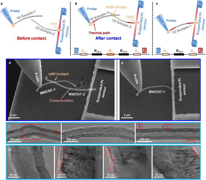
Before the two 1D samples come into contact, a parabolic temperature profile is established along the Pt nanofilm when applying a direct current, which allows us to calibrate the thermal conductivity of the Pt film. Upon contact between the two 1D samples, a heat pathway is established from the nanofilm to the heat sink through the 1D samples, which leads to a reduction in the temperature rise within the nanofilm. We measure the change in the average temperature rise of the Pt nanofilm from its temperature-dependent electrical resistance, from which we can extract the total thermal resistance of the two 1D samples in contact, denoted as Rt,tot. As illustrated in the thermal circuit in Fig. 1b, this total thermal resistance includes the thermal resistance of the two 1D sample segments in the heat path, denoted as R1D-1 and R1D-2, respectively, and the TCR between the two 1D samples, denoted as Rc, as well as the negligible TCR, Rcp and Rcs, at the well-bonded junctions between the 1D samples and the probe or the nanofilm sensor 29,30,31,32,33 . After the thermal measurements for all the contact morphologies, we separate the two 1D samples and measure the thermal conductivity of each sample using the same T-type method 29,30,31,32,33 , as illustrated in Fig. 1c, and thus obtain the thermal resistance of each sample segment, R1D-1 and R1D-2, in the TCR measurement. Then the TCR between the two 1D samples is determined by Rc = Rt,tot − R1D-1 – R1D-2. More details of the measurement method are provided in Methods and Supplementary Note S4.
Figure 1d shows the SEM images when two MWCNTs (MWCNT-1 and MWCNT-2) come into contact. Figure 1e presents the SEM image of MWCNT-1 during the in-situ measurement of thermal conductivity. As depicted in Fig. 1d, the two MWCNTs exhibit structural non-uniformity and their axes are not straight. Besides, there is an attached contaminant on MWCNT-2. The transmission electron microscopy (TEM) images shown in Fig. 1f demonstrates the abrupt variations in diameter, structural irregularities, axis bending, and impurity or contaminant adhesion on the MWCNT surface. High-resolution TEM images, as illustrated in Fig. 1g, further reveal the presence of amorphous carbon attachments on the MWCNT surfaces. Thus, even for the same pair of two samples, the precise contact morphology varies significantly, contingent upon the surface quality at the specific contact positions.
In our experimental setup, the probe is affixed to a movable manipulator (Kleindiek MM3A-EM), while the nanofilm sensor on a silicon wafer is separately integrated into the SEM (FEI Versa 3D DualBeam) platform. This deliberate separation allows for the real-time adjustment of the contact morphology, including the contact position, the crossing angle between the two CNTs in cross contact, and the overlapping contact lengths for the aligned-contact morphology. Furthermore, we deliberately maneuver the contact position to traverse surface contaminants present on MWCNT-2. We captured the SEM images of these diverse contact morphologies in-situ with high resolution while we measured the thermal transport across these single junctions. Upon the contact of two MWCNTs, we observed the emergence of a strong vdW force, which ensures the stability of the contact (see Supplementary Movie S1).
Figure 2a–c shows the schematic illustrations and the SEM images of three distinct contact morphologies: aligned-contact (a1 and a2), cross-contact (b1 to b7), and contact-through-contamination morphologies (c1 and c2). The aligned-contact morphology signifies a scenario where the two MWCNTs exhibit overlapping contact lengths within the SEM image. In this configuration, heat is conducted concurrently along each MWCNT while traversing the interface. Cross-contact morphology denotes a situation where the two MWCNTs are positioned in a crossed orientation in the SEM image. The crossing angle between the heat conduction segments of the two MWCNTs is θ. Figure 2 also provides schematic diagrams representing top and side views of these various contact morphologies. For all the contact morphologies, we define the thermal resistance of the entire overlapping region in the SEM images as the thermal contact resistance, as indicated by the red dashed box in the schematic illustration in Fig. 2.
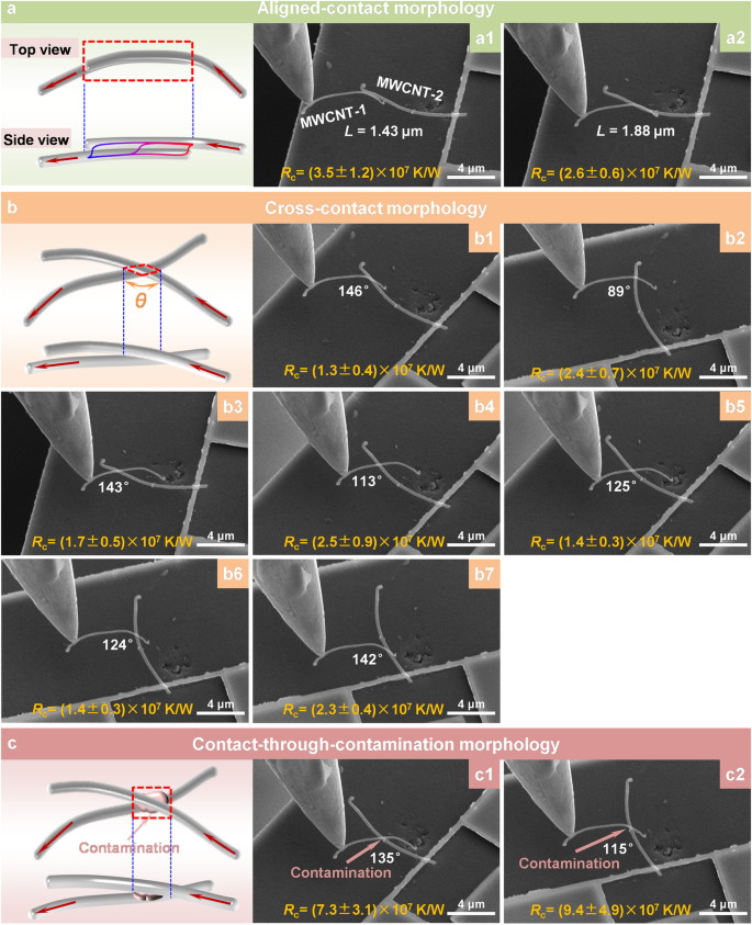
Figure 3a shows the difference in the average temperature rise of the nanofilm (∆T−∆TBL) after (∆T) and before (∆TBL) the contact for each contact morphology, from which the corresponding total thermal resistance is extracted (see Supplementary Note S4). Notably, this difference varies with distinct contact morphologies, with a lower ∆T − ∆TBL indicating a higher Rt,tot. The summary of total thermal resistance results for various contact morphologies is presented in Fig. 3b. Among these morphologies, the contact-through-contamination morphology exhibits a Rt,tot that is 2 to 4 times higher than the other two morphologies. After measuring the total thermal resistance, we separated the two MWCNTs and individually repositioned MWCNT-1 and MWCNT-2 to bridge the probe and the nanofilm sensor with EBID bonding, as depicted in Fig. 1e and the inset of Fig. 3c. Using the same thermal measurement approach, that is, comparing the change in the average temperature rise of the nanofilm after and before the bridging as shown in Fig. 3c, the thermal resistance of MWCNT-1 and MWCNT-2 was extracted as (6.18 ± 0.72) × 10 5 K W −1 and (1.19 ± 0.07) × 10 7 K W −1 with a suspended heat conduction length of 5.670 μm and 5.994 μm, respectively. From the TEM images shown in the Supplementary Note S3, the outer (Do) and inner (Di) diameters of the two samples were measured as (158.2 ± 9.3) nm and (73.3 ± 3.8) nm for MWCNT-1, and (240.0 ± 6.7) nm and (115.5 ± 11.3) nm for MWCNT-2. Then the shell cross-sectional area [A = π/4(Do 2 – Di 2 )] of MWCNT-1 (A1) and MWCNT-2 (A2) is calculated as (1.54 ± 0.17) × 10 4 and (3.47 ± 0.23) × 10 4 nm 2 , respectively. Furthermore, the thermal conductivity is extracted as λ1 = (594.8 ± 94.1) W m −1 K −1 for MWCNT-1 and λ2 = (14.5 ± 1.3) W m −1 K −1 for MWCNT-2. Notably, the TEM images reveal that the right end of MWCNT-2 exhibits more structural disorders, and it is part of the heat conduction segment. However, the amorphous end of MWCNT-1 is not included in the heat conduction segment. Consequently, the lower thermal conductivity of MWCNT-2 can be attributed to these structural defects. The uncertainty analysis is provided in Supplementary Note S7.
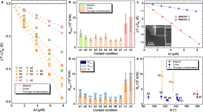
Taking into account the suspended heat conduction length of the MWCNTs in each contact morphology, we determined the thermal resistance of each MWCNT segments. Figure 3(d) delineates the distinct contributions of the two MWCNT samples and the contact to the total thermal resistance for all eleven contact morphologies. The thermal resistance of MWCNT-1 in the contact experiments is around 3 ~ 6 × 10 5 K W −1 , while its magnitude is around 10 7 K W −1 for MWCNT-2 due to its low thermal conductivity. The thermal contact resistance is denoted by the orange pillar in Fig. 3d and represented in the SEM images in Fig. 2. The aligned-contact and cross-contact morphologies exhibit comparable TCR. The TCR of aligned-contact morphologies a1 and a2 is (3.47 ± 1.16) × 10 7 K W −1 and (2.60 ± 0.56) × 10 7 K W −1 , respectively. For the cross-contact morphologies, the TCR varies with the specific contact conditions and its range is (1.31~2.51) × 10 7 K W −1 , the difference can come from the variable and irregular surface quality. The TCR of contact-through-contamination morphologies c1 and c2 is (7.27 ± 3.11) × 10 7 K W −1 and (9.36 ± 4.87) × 10 7 K W −1 , respectively, which is 3~7 times higher than the other two kinds of contact morphologies. Therefore, even for the same pair of two CNTs, the TCR across the single contact can vary by at least one order of magnitude depending on the specific vdW contact morphology. Figure 3e provides insights into the dependence of TCR on the angle between the two MWCNTs. For the cross-contact morphology, the observed dependence is weaker than suggested by some simulation studies 13,15 , as the actual samples exhibit inevitable defects that deviate from the ideal models used in simulations. The variations in the surface quality and crystalline structure within the individual CNTs can lead to distinct vdW interactions at the nanoscale interfaces and thus significantly influence interfacial thermal transport.
Figure 4a delineates the schematic diagram illustrating the principles governing thermal transport in an ideal aligned-contact junction, where two 1D samples have an ideally aligned contact segment with an overlapping contact length of L. The heat flows along 1D sample-2, crosses the interface at the aligned contact segment, and concurrently flows along 1D sample-1. Note that the previous study 18 approximated TCR by treating the aligned contact as a cross contact located at the midpoint of the overlapping segment. However, this approximation can cause large uncertainty when the overlapping contact length is very large or the thermal resistance within the CNT is much larger than the interfacial thermal resistance (see Supplementary Note S5). Here, we define the interfacial thermal conductance per unit length between the two CNTs, denoted by g, which should be a constant along the contact length for uniform contact conditions. We established the heat diffusive model for both CNTs, the differential equations, boundary conditions and analysis details of which are provided in the Supplementary Note S5. From this heat diffusive model, we can solve for the temperature distribution along 1D sample-1 (T1) and 1D sample-2 (T2). This analysis enables the derivation of the relationship between TCR and g, λ1, and λ2 as follows,
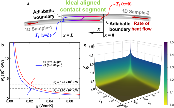
Figure 4b illustrates the Rc versus g curves after we substituted the parameters of two tested aligned-contact morphologies. For morphology a1 whose Rc is equal to 3.47 × 10 7 K W −1 , the corresponding g is 0.0207 W m −1 K −1 . For morphology a2 whose Rc is equal to 2.60 × 10 7 K W −1 , g is 0.0216 W m −1 K −1 . In some simulation studies, the g between two single-walled carbon nanotubes (SWCNT) with an overlapping length of nanometers is around 0.06 W m −1 K [−116,34,35 . In our study, the contact may not be perfect along the overlapping segment.
We further define two dimensionless figures, denoted as t1 = λ1A1/(gL 2 ) and t2 = λ2A2/(gL 2 ), representing the ratio of thermal conductance of two samples and the interfacial thermal conductance at the aligned-contact segment, then Eq. 1 can be expressed as follows,
$$RcgL is the ratio of the TCR to the interfacial thermal resistance for the aligned-contact morphology. Figure 4c shows the dependence of RcgL on t1 and t2. Given that Rc encompasses not only interfacial thermal resistance but also the thermal resistance of the two samples within the aligned contact segment, RcgL consistently exceeds 1. Additionally, as either t1 or t2 decreases, RcgL exhibits an increasing trend, and RcgL will also be influenced by the relative ratio of t1 and t2. The tendency for RcgL to increase is more pronounced at lower values of t1 and t2. For our tested aligned-contact morphologies a1 and a2, RcgL is 1.028 and 1.055 respectively.
Understanding TCR per unit contact area is fundamental in elucidating the intricate mechanisms governing interfacial heat transfer, so it holds significant importance to define and calculate the contact area. Whereas nanoscale contact area concepts remain ill-defined, and the diversity of contact morphologies complicates the quantification of contact area. The calculation process necessitates: (1) the selection of a criterion for identifying which atoms are in contact, (2) a method for identifying atoms that meet this criterion, and (3) the conversion from the number of atoms in contact to the contact area 36 . Different definitions of the contact area can significantly impact the results in both experiments and simulations.
In our experiment, what we can directly measure is the overlapping area between the two cross-contacted MWCNTs from the SEM images. However, it is considerably higher than the actual vdW contact area, which is determined by the vdW interaction between the two MWCNTs. When the attractive and repulsive vdW forces between atoms near the interface are balanced, the two MWCNTs reach a dynamic equilibrium with an equilibrium distance between them 36 . Besides, since vdW interaction is short-ranged, its contribution becomes negligible once the distance between the atom pair exceeds a certain cutoff distance. Given that MWCNTs comprise multiple layers of carbon atoms, the interactions between numerous pairs of atoms construct a three-dimensional (3D) potential energy field space 37 . For cross-contact morphology, the contact area can be calculated utilizing classical theoretical models such as the Johnson-Kendall-Roberts (JKR) theory (see Supplementary Note S6) where the interaction between two perpendicularly crossed cylinders is conveniently regarded as the interaction of a sphere with a plane 38,39 . Nevertheless, this assumption of simple pairwise additivity inherent to these models disregards the influence of neighboring atoms on the interaction between any pair of atoms. Furthermore, it is not suitable for calculating the contact area of the aligned-contact morphology whose θ is 180°, rendering a universal description of TCR per unit contact area (Rc,ca) for different contact morphologies unattainable.
Based on the above discussion, we propose a straightforward assumption to estimate the contact area for both cross-contact and aligned-contact morphologies. Figure 5a and b presents the schematic illustrations, using a cross-contact morphology at a right angle and an aligned-contact morphology as examples. An equilibrium distance of 0.24 nm 37 is assumed between the two MWCNT samples. The vdW interaction space for each MWCNT sample is considered independently, and radii are extended along the axes of each MWCNT by a cutoff distance (which we take as 1 nm) 12,18 to construct two transparent cylinders at the contact position. A 3D overlapping space exists between the carbon nanotube and the transparent cylinder of another carbon nanotube, representing the portion of this nanotube subject to the vdW action of the other nanotube. Similarly, there is also a 3D overlapping space between another nanotube and the transparent cylinder of this carbon nanotube. The average of the projected areas of these two 3D overlapping spaces is calculated and denoted as (Athe), treated as the contact area. For the aligned-contact morphology, the contact width can be further extracted.
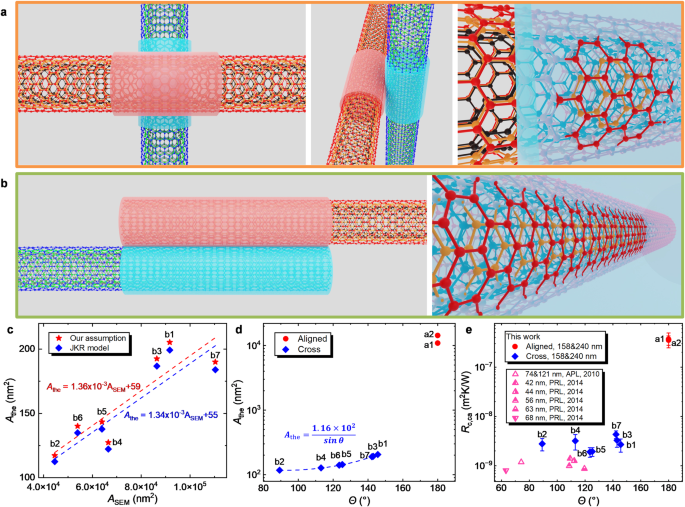
Leveraging the geometric parameters of the two MWCNTs and the angle between them, 3D models are built to measure the average of the projected area of the 3D overlapping spaces. Figure 5c shows the measured contact area for the cross-contact morphologies, the contact area is 117~205 nm 2 and corroborates with the values calculated by JKR theory (see Supplementary Note S6). Notably, this contact area is two orders of magnitude lower than the overlapping area between two MWCNTs in the SEM images (ASEM). Moreover, Athe exhibits a linear relationship with ASEM, enabling a rough estimation of contact area based on overlapping areas in SEM images. The deviation in linearity arises from SEM images being two-dimensional, while carbon nanotubes exhibit three-dimensional curvature, with their diameters varying along the axial direction. Figure 5d further shows the contact area calculated from our assumption for both cross-contact and aligned-contact morphologies with respect to θ. For the cross-contact morphologies, the contact area is proportional to 1/sinθ. For the aligned-contact morphologies, the acquired contact width measures 7.6 nm and the contact area for a1 and a2 is 10916 nm 2 and 14315 nm 2 respectively, which is 50 ~ 100 times higher than that of the cross-contact morphologies, primarily due to the long overlapping contact length.
The TCR per unit contact area for various contact morphologies is summarized in Fig. 5e. At the contact region, since only several outer walls of MWNTs play a dominant role in the vdW interaction 37 , and the surface quality (defects, disorders, impurities, adhesion, and so forth) along the tube is not uniform, even for different cross-contact morphologies Rc,ca is also different and its range is (2~4) × 10 −9 m 2 K W −1 . Experimental results of Rc,ca for cross-contact between two MWCNTs with different diameters from the only two references 18,19 are also given for comparison. Note that the authors of refs. 18,19 . were not able to measure the thermal conductivity of each sample in the fixed contact, which could cause large uncertainties. For the aligned-contact morphologies a1 and a2, Rc,ca is (3.68 ± 1.23) × 10 −7 m 2 K W −1 and (3.53 ± 0.76) × 10 −7 m 2 K W −1 , respectively. The two-orders-of-magnitude higher value than the cross contact is attributed to the uneven quality of contact across all the overlapping lengths in the aligned contact. The unavoidable non-uniform surface crystallinity during the synthesis of MWCNTs 40 , coupled with the deformation of the 1D samples, which can lead to irregular interfacial spacing, can contribute to the higher average TCR per unit area across the overlapping contact segment.
We have developed an in-situ SEM approach that enables a precise correlation between the interface thermal transport across two CNTs and the nanoscale contact morphologies. We employ a nano-manipulator to vary the overlapping lengths, contact positions, and crossing angles between the same pair of multiwalled CNTs, and concurrently measure the thermal contact resistance (TCR) at the adjustable single vdW junction using a suspended MEMS thermal sensor. The measured TCR varied significantly with the contact morphologies, spanning an order of magnitude even within the same pair of samples, which can be attributed to the uneven intermolecular force distributions, effective contact areas, and structural non-uniformity. The highest TCR was measured for contacts involving nanoscale surface contamination. For the aligned-contact morphology, we established a general heat diffusive model for 1D materials that was previously lacking. The extracted interfacial thermal conductance per unit length between the MWCNTS was approximately 0.02 W m −1 K −1 regardless of the contact length. Furthermore, we proposed a unified definition of the vdW contact area for both the cross-contact and aligned-contact morphologies. The TCR per unit vdW contact area averaged approximately 3.60 × 10 −7 m 2 K W −1 for the aligned contact morphologies, which is two orders of magnitude higher than that for the cross-contact morphologies. This significant difference can be attributed to the non-uniform contact quality along the aligned contact segment, as evidenced by real-time SEM images. Our work presents an in-situ measurement method and a unified analysis approach to understand the influence of intricate nanoscale contact conditions on interfacial thermal transport between 1D and even 2D materials. This study can provide guidance for controlling heat in various applications, such as the development of thermally conductive composite materials, thermal management in nanoelectronics, and thermoelectric energy conversion.
The suspended Pt nanofilm sensors were fabricated by a series of MEMS fabrication processes including electron beam lithography, electron beam physical vapor deposition (PVD), and the etching processes (see Supplementary Note S1). The thickness of the Pt thin film was 40 nm. An 8-nm-thick titanium layer was used for adhesion between Pt and SiO2 during the PVD, and then etched off by buffered HF etching along with SiO2. Subsequently, the Si substrate was etched using CF4 plasma, leaving the Pt sensors suspended above the substrate, followed by O2 plasma to increase the insulation of the Si substrate. The Pt nanofilm sensors also underwent the annealing treatment to improve the grain condition. From the SEM images, the length and width of the sensor used in the TCR measurements and the thermal conductivity measurement of MWCNT-2 are measured to be 9.737 μm and 367 nm, the length and width of the sensor used for the thermal conductivity measurement of MWCNT-1 are 9.820 μm and 358 nm, respectively.
The MWCNTs in the powder form (Hodogaya Chemical Co., Ltd.) were added to acetone, and sonicated until suspended. Subsequently, a drop of the suspension was deposited on a TEM grid (Gilder Cu G-2000HS, Okenshoji Co., Ltd.) and left to dry in a vacuum chamber. The structure characterization was conducted with a TEM (JEM-2100Plus, JEOL) operated at 200 kV. We punched a hole in the TEM grid to locate the sample in SEM by the position of the sample relative to the hole.
Since the Pt nanofilm sensor is used as a resistive thermometer, prior to the thermal resistance measurements, we calibrated the electrical resistance-temperature dependence of the nanofilm sensor at 278.15 K, 298.15 K, and 318.15 K (see Supplementary Note S2) for further measuring its thermal conductivity 11,30 before each contact between the two MWCNTs. In the calibration measurement, the silicon wafer with the nanofilm sensor was fixed on a Peltier stage which was mounted on the SEM sample platform.
During the thermal resistance measurements, the silicon wafer with the calibrated nanofilm was fixed on a holder that then was mounted into the SEM sample platform. The manipulator probe with the CNT attached was fixed on the SEM chamber wall. Before each vdW contact, we individually calibrated the thermal conductivity of the sensor. The calibration results of a total of eleven contact conditions, provided in Supplementary Fig. S8, ranged from 59.59 ± 0.28 W m −1 K −1 to 59.88 ± 0.27 W m −1 K −1 ,·exhibiting neglectable change during the whole measurements. On the SEM sample platform, there are two circuit interfaces for the manipulator and external measurement, respectively. In the external measurement circuit, we utilize a DC current source (Advantest R6243), two high-precision digital multimeters (Keithley 2002, 8.5 digits), and a standard resistor (Yokogawa 2792) to detect the current and voltage across the Pt sensor. More details can be found in the Supplementary Note S4 and refs. 11,41 . We also captured the deformation dynamics of the two MWCNTs during the detachment process, revealing the presence of a strong vdW force. The corresponding video is provided as Supplementary Movie S1.
The data that support the findings of this study are available from the corresponding author upon reasonable request.
We thank Professor Yasuyuki Takata for providing the FEI Versa 3D DualBeam instrument, and Mr. Tatsuya Ikuta and Dr. Takanobu Fukunaga for the maintenance of the experimental equipment. D. Li thanks the China Scholarship Council for financial support. This work was partially supported by the JST FOREST Program (Grant number JPMJFR212M, Japan), JSPS KAKENHI (Grant nos. JP23K26053 and JP24H00293), and the JST CREST Grant number JPMJCR18I1, Japan.